Great 32 Channel ADC card.
Single channel ADC card sub-module definition.
Sub-module ADC card Signals.
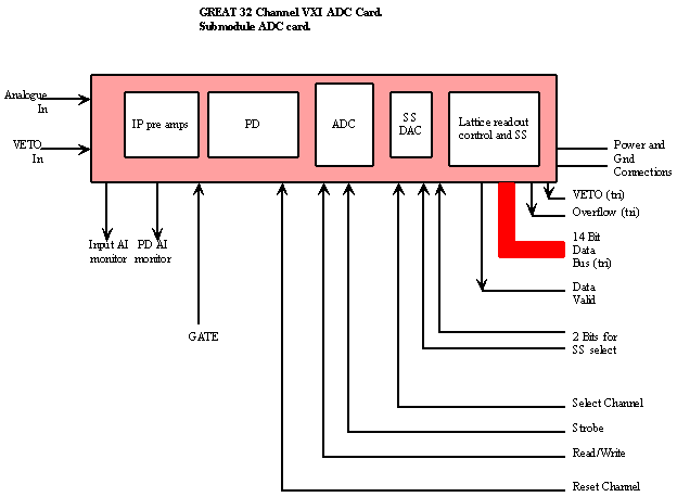
Figure 1 ADC card interface signals
Basic components and functions.
- Input Preamps
- Peak detector
- ADC including SS subtraction circuit
- DAC for SS
- Lattice readout chip for control of readout and SS subtraction.
1. The input preamps buffer the signal from the input cable and provide a low impedance signal out for the Peak Detector.
2. The included Peak Detector (PD) is controlled from the lattice chip. The ADC convert signal is generated from the end if the GATE period.
3. The ADC is 14 bits with a SS circuit controlled by the ADC data valid flag on the card. When the DV flag is set the SS increments. The valid data will have been latched in the Lattice chip output registers by this point.
4. The DAC is used for the SS offset on the ADC and has 256 levels (8 bit).
5. The Lattice chip has several tasks as follows.
a) To act as the SS controller for the DAC/ADC.
b) To accept the ADC data, subtract the SS value and register the data in output buffers.
c) To detect any data overflow within the ADC when the SS system is turned on, such that bad data would be generated.
d) To detect a VETO input occurring during the time from the Gate Start up to Data Valid, setting a VETO flag in the data output. (Note - Pile up is controlled and registered by the time stamp chip, external to the ADC).
e) To generate the convert signal for the ADC from the end of the Gate.
f) Decoding the Channel select signal with the Reset, read/write, Strobe etc. for control of the module as required.
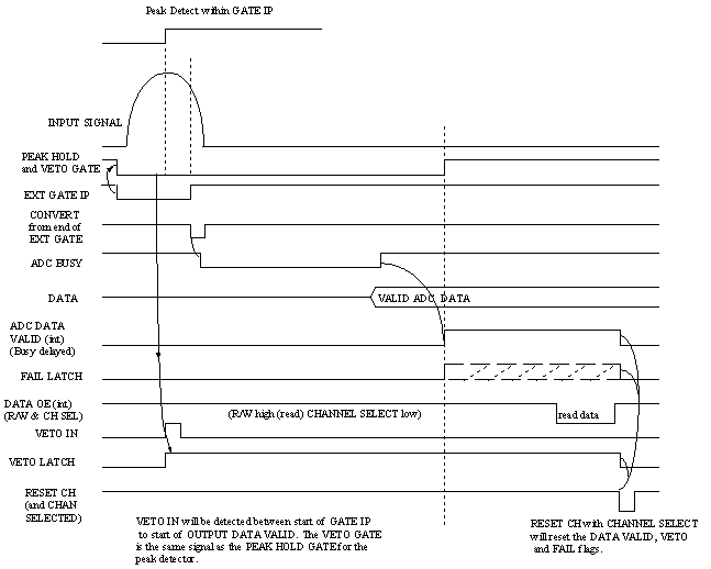
Figure 2 Timing internal to ADC channel
Description of signals
|
SIGNAL |
DESCRIPTION |
Signal type |
H action |
L action |
|
Analogue
input |
Unipolar
or Bipolar shaped signal |
Individual |
- |
- |
|
VETO
in |
VETO
this event (within Gate to DV time only) TTL from Timestamp sub module. |
Individual |
- |
- |
|
Input
inspection line |
Analogue
inspection monitor of input signal |
Individual |
- |
- |
|
PD
Inspection line |
Peak
detector monitor point |
Individual |
- |
- |
|
Gate |
TTL
signal to open the PD gate. Input analogue signal must peak before gate
closes. Width controlled by chip on Timestamp sub module. |
Individual |
None |
Open gate |
|
14
bit data/address bus |
Bus
for reading Data from the ADC. |
Common |
1 |
0 |
|
VETO
status bit |
Set
if a VETO input was detected within
gate start to DV period. Tri-state read out with data. |
Common |
VETO |
No VETO |
|
FAIL |
Set
if ADC goes out of range or SS overflows. Tri-state, read out with data. |
Common |
Overflow |
Normal |
|
Data
Valid (DAV) |
Set
when data is valid after SS subtraction. |
Individual |
Valid |
Not valid |
|
Mode
bits (2) (SS0
SS1) |
(SS ON,FS,Zero). Latched on ADC module by
Strobe + Channel Select + Write. Used for SS on/off and full/zero scale. |
Common |
1 |
0 |
|
Select
Channel |
Selects
ADC channel being addressed. From Time stamp sub module. |
Individual |
None |
Enabled |
|
Strobe |
Strobe
used to write SS0 SS1 values to register. Data written on back (rising) edge
of strobe. |
Common |
None |
Valid |
|
Read/Write |
Read/write
select. |
Common |
Read |
Write |
|
Reset |
Clears
data valid and status bits (With Select Channel signal) |
Common |
None |
Clear |
|
Power |
Power
supplies as required. (+/-15V,+/-12V, +/-5V) |
Common |
- |
- |
Signal Timing
|
Signal
|
Timing |
|
OE
command (!W + CS) to output valid |
17ns
max |
|
Clear
to DAV false |
20ns max |
|
|
|
|
|
|
Sliding
Scale Codes
|
SS1 |
SS0 |
ACTION |
|
0 |
0 |
SSON |
|
0 |
1 |
SSOFF (HELD AT ZERO) |
|
1 |
0 |
SS FULL SCALE ADJUST (offset applied to ADC but not subtracted) |
|
1 |
1 |
SS ZERO SCALE ADJUST (no offset applied to ADC (same as 0 1 above) |
NOTE:-
The input voltage to the ADC card must be in the range 0 to 8V (8V approximately). It must be positive with respect to ground. The Peak detector will only operate with positive inputs and erroneous ADC codes will be generated should the ‘peak’ happen to pull the input below ground.