05/07/2000
Exogam Project
GIR
V5 MAP
for
E.S.S.
Card
Ver
1.1
By: I. Merlin, N. Karkour
(C.S.N.S.M. Orsay)
In collaboration with:
I. Lazarus (NPSG UK)
1. Description
of the G.I.R.V5 for the E.S.S. card.......................................................................... 2
1.1. Exogam
Detector:................................................................................................................... 2
1.2. DSP
online data processing:................................................................................................... 2
1.2.1. Multiprocessing
Control:..................................................................................................... 2
1.2.2. Power
Supplies Control and automatic Pole Zero Adjustment............................................. 2
1.2.3. On-Line
Histogrammer and Datas Processing..................................................................... 3
1.3. Readout
Mechanism:............................................................................................................... 3
1.4. Electrical
and Mechanical precautions:................................................................................. 4
1.5. ESS AP Description............................................................................................................... 5
1.5.1. General
description............................................................................................................ 5
1.5.2. Detailled
description........................................................................................................... 6
1.5.3. Pinouts of the AP Connector for the ESS Card................................................................. 9
2. Memory
Map of the GIRV5 for the ESS Card........................................................................ 10
2.1. VXI
Configuration Registers................................................................................................. 10
2.2. Common
Register Area......................................................................................................... 10
2.2.1. GIR
Module Control Register : GMCR........................................................................... 11
2.2.2. ESS
Module Control Register : EMCR............................................................................. 11
2.2.3. Inspection
lines................................................................................................................. 11
2.2.4. Temperature
Control Register........................................................................................... 15
2.2.5. DAC
Buffer settings......................................................................................................... 16
2.2.6. GIR
Readout Control and Status register area................................................................... 16
2.2.7. GIRV5
Readout Control Register : RCR......................................................................... 17
2.2.8. GIRV5
Readout Status Register....................................................................................... 17
2.2.9. Readout
Setup Area......................................................................................................... 17
2.3. Channel
Area Addresses....................................................................................................... 19
2.3.1. DAC
Setting Registers:..................................................................................................... 20
2.3.2. CCR
Definition................................................................................................................ 20
2.3.3. Time
Alignment Registers................................................................................................. 21
2.3.4. TDC
Control Registers..................................................................................................... 21
3. General
figures........................................................................................................................... 23
3.1. GIRV5
Card Dimensions....................................................................................................... 23
3.2. PCB_AP
board connections:................................................................................................ 24
3.3. GIRV5
Shift registers connection figure............................................................................... 24
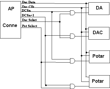
3.4. GIRV5
Dac and potentiometer connection figure................................................................ 24
1.
Description of
the G.I.R.V5 for the E.S.S. card.
1.1. Exogam Detector:
One of the solutions for electronics of the
data acquisition systems in Nuclear physics experiments is to use VXI (VME eXtension bus for
Instrumentation) standard electronics.
In EXOGAM
we have new detectors called the Segmented
Clover detector. Each detector contains 4 central contact Ge crystals, and 16 outer contact
crystals with its escape suppression shields (made of BGO)at the sides, and
Caesium Iodide (CSI) as back-catchers. We have 4 Clover shields in one VXI card
: ESS Card (EXOGAM Suppression Shield). Each shield delivers 4 outputs from the
BGO and 4 outputs from the CSI. GIRV5 assumes the analogue part configuration,
the Readout interface logic (internal, and external), the VXI power supply filtering, the Inspection lines control logic, the
DSP control for online data
processing. Connections between GIRV5 and ESS card is done by 3 AP connectors
with 150 pins each.
GIRV5 was accepted because it responds to the
request, and the constraints asked for the ESS
card. The GIRV5 is a Readout
Interface card, which is connected between the VXI back plane and the ESS
Analogue card, so that the 2 cards (GIRV5-Analog) form a complete VXI D-size Board. This Board have
programmable Input/ Output signals that are connected to the Analogue cards to setup and configure
the registers, and thresholds as well as data acquisition parameters for EXOGAM.
The GIRV5
's job is to read out the corrected ADC
data and writes them (or not) into the FIFO's,
then these data are transferred to the VRE
(VXI Readout Engine) Board on the VXI
back plane. The Readout mechanism is completely programmable, and suitable for
any acquisition system. In the case of EXOGAM,
Eurogam Readout interface for common
deadtime is used.
1.2. DSP online data processing:
1.2.1.
Multiprocessing
Control:
This new feature is added to interconnect any
assembly of VXI cards DSP's together through the VXI Local bus. This feature is
completely programmable. That is by software control we can specify graphically
which VXI cards can be grouped
together through the Local bus, so that the DSP
can have data exchange for Readout decision, and in this way we can decide in a
more accurate way if the data in the FIFOs
are good data or not. In another context, this decision acts as a trigger level
which could be called Readout trigger, that is after the data are sent
to the FIFO's the DSP can make some analysis on these
data, and can interrupt the external Readout cycle if those analysis don't
correspond to what the user needs.
1.2.2. Power Supplies Control and automatic Pole Zero
Adjustment.
Other feature for the DSP is Local control on the VXI
card for Analogue signal through a 16 input Analogue multiplexer; there are 2
free Analogue flags on the AP connector, the Analogue Inspection Lines as well
as the Voltage inspection line are connected to this multiplexer, and the VXI
power supplies are connected too. We can, for example, control the power
supplies and send flags when their level go up the references.
We can also control the Automatic Pole Zero Adjustment specific for Ge detectors or other detectors which
need Pole Zero Adjustment or other Automatic Dac Adjustment (by DSP Programming). This multiplexer is
connected to a local high Speed 66MHz Flash ADC,
then the values are written in the DSP
RAM, after which the DSP Processes the data, and send the
correction to the Software on-line
control through flag registers.
1.2.3.
On-Line
Histogrammer and Datas Processing.
DSP process ADC data and builts spectra in its external memory (Spy mode). DSP can also process datas (gain adjustment) before sending them to FIFO (Filter mode). The external memory can store 64 spectra of 14 bits.
Spy mode: In this mode the DSP just collects the data at the same time, as they go onto the VXI backplane, during an event and make
processing on these data, and puts the result in its Memory. This can help the
user to check on the results inside each card during an experiment to make sure
that the card setup is done good. The DSP
DOES NOT make any modification on the good data .
Filter mode: The GIRV5 can be programmed by software to make the DSP read the data without sending it to
the VXI backplane, and then the DSP, automatically, makes data
processing, and sends back the results to GIRV5
readout interface which sends it back to the VXI backplane. In this mode the DSP
can make any kind of filtering on the data, and even keeps the raw results, and
add more processed data inside the same event. This method can help the user to
get more information from each event in addition to the raw data.
1.3. Readout Mechanism:
The Readout Mechanism will be divided into two
cycles: Internal, and External Readout cycles. The Internal cycle is the cycle
which takes place for data transfer between the Analogue card, and the GIRV5.
While the External Readout cycle is the interface between the G.I.R, and the VRE Board.
In the External Readout cycle the Eurogam Readout interface will be used.
We will upgrade later the Readout interface to several Readout mechanisms due
to programmable devices (e.g. SSBLT
or MBLT 64 transfer etc.).
In EXOGAM the GIRV5
uses as in Eurogam the same VXI lines dedicated for the Digital, and Analogue multiplexing lines, Fast
trigger, and Validation signals,
etc...
First, When the CFD of a Ge channel fires
and when the Sumbus signal exceeds
the sumbus threshold in the MASTER trigger, this latter sends a Fast Trigger
signal followed by a Validation
signal (with the event no. on the VXI
local bus) as a confirmation that the present event (which is already running)
is a good event to be coded, and the data in the ADCs are to be read out or
transferred into the FIFO[1].
When it receives Validation the VRE
asserts the AS* (Address Strobe)
signal onto the VXI back plane with
the event no. on the VME address bus,
and waits for the VXI boards that
participate in this event by asserting or not BLTACK* (BLTACK* is an
open collector signal). At that time the Readout interface inside each GIRV5 maintains BLTACK* if Validation Acknowledge signal from the Local Trigger(s) is asserted, and it waits until the ADC data are sent out to the FIFO.
The VRE reads all the data from all
the VXI cards by daisy chain[2].
For more details about how the GIRV5
builds its interface refer to the Readout
document, concerning both the Internal, and the External Readout mechanism.
1.4. Electrical and Mechanical precautions:
This card is specifically designed for low
noise Analogue data acquisition systems. It takes care of the EMC problems. It already contains
several elements which worked before in other similar cards. Data transfer is
20 Mbytes/sec 5 Mwords/sec, and in Nuclear
physics data acquisition systems the shaping time and the coding time take
highest percentage of the total channel dead time.
The aim of this Board is to have Readout interface completely programmable for different Readout mechanisms, and which can be suitable for different data acquisitions. That is it can be adapted to either fast or slow data transfers. The Analogue engineer need not be anxious about the Readout part of his Board. He needs only to design his Board up to digital data, and then he has to choose the Readout system to be adapted for his experiment, so that the Readout interface can be built.
EMC problems are very dangerous to sensitive
Analogue signals, especially in Nuclear
physics data acquisitions. GIRV5 has
the middle column of the 150 pin AP
connectors (as shown previously) mostly grounded. Extra flat connectors will be
used to minimise the electromagnetic noise penetrations. Slow asynchronous data
transfer from the FIFO's. (see the PCB_AP connections diagram.). For
example the 2 Analogue Inspection
Lines are surrounded with ground pins. Power Supply chokes, and OSCON capacitors are used to filter the VXI power supplies.
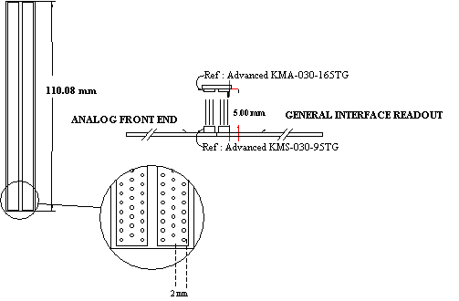
The interconnection between the Analogue card and GIRV5 can be shown in the figures below showing the top, bottom,
and face views. An extractor tool is built to extract the PCB_AP connector (450 pins) out of both the GIRV5, and the Analogue card.
A special tool exists to mount, and unmount the GIRV5, and the Analogue card
together with the PCB_AP without
having any pressure on the SMD
components, just on the surrounding of both PCB's
(see the mechanical dimensions, & the isometric view figures for more
details).
A new mechanic has been adopted to protect cards from high temperature and EM perturbations. The card is now fixed on 2 rails (upper and lower) and the whole is inserted in the crate slot. This has induced the decrease of the PCB dimensions, but the manipulation of the card during prototype tests is easier and safer. The rails are pierced with 450 holes each, increasing the airflow area about 50%. 2 shields are fixed by 36 screws in the rails, avoiding the alignment problem causing by the passage through the PCB in the old mechanic. EMC performances are above 90dB
1.5. ESS AP Description
The GIRV5
is connected to the Analogue card
through three connectors (3 x 50= 150 pins). These connectors are called Analog_P (AP) connectors. The connections between the GIRV5, and the Analogue card
is made through a PCB (called the PCB_AP).
The middle column of this connector is mostly connected to the ground for EMC precautions (for more details refer
to the Electrical Precautions).
These connectors are called AP1, AP2,
& AP3 ( from top to bottom). All three connectors are fully compatible
so that the same PCB_AP is used. For example the same power supply pins are
connected through a routing shape. Table 1 describes the three AP connector
pins, and their locations.
1.5.1. General description.
AP1:
a.
76 Input/ Output
pins (called Reg_Io) which are fully programmable pins of a XILINX FPGA
b.
10 bits of a
latched address bus (ADD 1 to ADD 10).
c. Filtered -2 volts VXI power supply.
d. 1 Analogue
Flag free signal which is connected to an analogue multiplexer inside the
GIRV5, and which can be digitised by the DSP program, plus two digital free I/O
signals(RDFLAG1,2).
AP2:
a. The higher 16 bit of a latched address bus (ADD 11 to ADD 23).
b. There is also the Analog, Digital, and
Voltage Inspection Lines which come from the Analogue card.
c. the lower 16 bits of the bidirectional data
bus.
d. 16 input/output reprogrammable pins (called
Reg_Io) from XILINX FPGA (LCA Decode2).
e. 18 input/output pins from the ReadOut LCA (READ 0 to READ 17 except READ 6,8,10,11,14 which are buffered
output signals to the Analogue card.
f. 4 TTL
signals which come from the VXI back
plane as ECL signals (they are the Trigger Event numbers in EXOGAM ),
g. 1 Analogue
Flag free signal which is connected to an analogue multiplexer inside the
GIRV5, and which can be digitised by the DSP program, and two digital free I/O
signals (RDFLAG3 ,4).
AP3:
a. The higher 16 bits of the data bus (DATA 16 to DATA 31).
b. 5 input/output signals from the ReadOut LCA (READ 18 to READ 22).
c. The Differential VXI line Starx +/- , and 2 TTL
Trigger lines (which is the Fast Trigger, Validation, and Inhibit
signals respectively). They are the EXOGAM
MASTER Trigger signals.
d. Moreover there are 49 INPUT/output pins from
LCA Decode2 (called Reg_IO).
e. 4 bits which are connected to the highest
nibble in the FIFO, they are the event no.
latched in the Analogue Board.
f. 3 TTL signals which can be used as flags for
the DSP
g. the VME
16 MHz Clock, and filtered +/- 12 volts
VXI power supply.
1.5.2. Detailled description.
1.5.2.1.AP1 :
-
Ddin : serial data signal to load the DACs,
this signal is common for all the Dacs.
-
DClk : clock signal to load the DACs,
this signal is common for all the Dacs.
-
DCSA n : Chips Select for threshold DACs on channel n (n=0,1,2,3).
-
DCSB n : Chips Select for Local Trigger DACs on channel n (n=0,1,2,3).
-
CCR n[3:0]: 4 bits Channel Control
Register for channel n (n=0,1,2,3).
-
Bgo q-wr : BGO q_Align_Delay_WrEn signal for quadrant q (q=A, B, C, D).
-
Csi q-wr : Csi q_Align_Delay_WrEn signal for quadrant q (q=A, B, C, D).
-
Ge q-wr : Ge q_Align_Delay_WrEn signal for quadrant q (q=A, B, C, D)
-
TDC q, 5 : TDC_Stop_Select signal for quadrant q plus one common (q=A, B, C, D)
-
VetoDelay : Veto_Delay_WrEn signal.
-
VetoWidth : Veto_Width_WrEn signal
-
Pattern : Pattern_Delay_WrEn signal.
-
MyChSel n : Select the channel (detector) for Alignment, TDC, Veto and Pattern
(n=0,1,2,3).
-
RgiSel : Indicates a VME cycle with valid AM code for address in range 0x400 to
0xFFE (Readout Setup Registers).
-
RegStrobe : Latch VME data into RGI registers.
-
LI 1,2_En n : Enable the digital inspection lines 1 and 2 on
channel n (n=0,1,2,3,4).
-
Digstrobe 1,2 : Latch data to select parameter on digital
inspection lines 1 and 2.
-
AI 1,2_En n : Enable the digital inspection lines 1 and 2 on
channel n (n=0,1,2,3).
-
AIstrobe 1,2 : Latch data to select parameter on analogue
inspection lines 1 and 2.
-
ADD[10:1] : this is the lowest byte of the VME
Address bus, it is enabled by the GIRV5
- Temp
Led : ON if Over or under normal temperature.
- Error
Led : ON if Fifo Error.
- Done
Led : ON if all LCAs are
programmed.
- VPTAT
1 : Temperature Monitoting Sensor 1.
-
+5 V : 6
pins.
-
-5.2 V : 6
pins.
- -2 V : 8
pins.
1.5.2.2.AP2 :
-
Clk 33MHz :
- Last
Pass : Renout of the analogue
card indicates end of readout cycle.
- StartRdt
: This signal is the
Start_Readout of the analogue card, which is the back edge of the last Busy signal.
- Valack
: this signal is the Validation Acknowledge given by the last (Daisy chain) Local Trigger.
- Dtready
: Signal given by analogue
card when a data is ready to be latched
on the bus.
- Renin
: Start readout cycle of
events, this signal is sent by GIR to the analogue card.
- AI 1,2 :
Analogue Inspection Lines 1 and 2.
- DI 1,2 :
Digital Inspection Lines 1 and 2.
-
ADD[23:11] : VME Address bus, it is
enabled by the GIR
- DATA[15..0]
: these bits are the 16 LSB GIR Data bus. This bus has 2 functions :
it is the VME data bus during
read-write operation of the analogue card and GIR DSP data bus during Readout.
- EvtIn
[3:0] : 4 bits Event Number from Lbus.
- EvtAna
[3:0] : 4 bits Event Number to GIR Readout
- L[0:7] : Local Data bus used for setup LI and AI lines, alignments delays, veto,
pattern adjustments, TDC control
- EMCR
[3:0] : 4 bits ESS Module
Control Register.
- LTResetGir
: This signal indicates the
end of the event processing. It goes to the
analogue card which sends it to the
Local Triggers that were read out.
- Dtack
: buffered data acknowledge
signal for each word of the the analogue
card in readout cycle.
- Global
Reset : buffered global reset
signal.
- Clk16MHz
:
- OVER
1,2 * : Indicates over
temperature for sensors 1 and 2
- UNDER
1,2 * : Indicates under
temperature for sensors 1 and 2
- +5 V : 6 pins.
- -5.2
V : 6 pins.
-
+12 V : 4 pins.
- - 12
V : 4 pins.
1.5.2.3.AP3 :
- DATA[31..16]
: these bits are the 16 MSB GIR Data bus. This bus has 2 functions :
it is the VME data bus during
read-write operation of the analogue card
and GIR DSP data bus during Readout.
- R/W :
buffered VME read-write signal.
- Inhibit*
: buffered Inhibit signal from the MASTER Trigger (on the VXI back
plane). It is used by Local Triggers only
when singles are disabled.
- Fast
Trigger : buffered Fast Trigger
signal ( positive TTL ) from the MASTER Trigger (starX +/- on the
VXI back plane).
- Val*
: buffered Validation signal from the MASTER Trigger (on the VXI back
plane).
-
Beam RF : Beam signal
- PromCS
: serial PROM Chip Select
signal of the ESS Analogue card.
- PromRd: serial
PROM Data to be read out of the ESS
Analogue card.
- PromWr: serial
PROM Data to be writen of the ESS
Analogue card.
- Promhd: Hold
signal for serial PROM of the ESS
Analogue card.
- DSPFLAG
1to 3 : TTL signals which can
be used as flags for the DSP
- VPTAT
1 : Temperature Monitoting Sensor 1.
- +5 V : 6 pins.
- -5.2
V : 6 pins.
-
+24 V : 4 pins.
-
-24 V : 4 pins.
1.5.3. Pinouts of the AP Connector for the ESS Card
|
|
AP1 Connector |
AP2 Connector |
AP3 Connector |
|
||||||
|
|
ROW A |
ROW B |
ROW C |
ROW A |
ROW B |
ROW C |
ROW A |
ROW B |
ROW C |
|
|
1 |
+5
V |
+5v |
+5v |
+5
V |
+5
V |
+5
V |
+5v |
+5v |
+5v |
1 |
|
2 |
DDIN |
GND |
DCLK |
Clk33Mhz |
GND |
ADD
11 |
DATA
16 |
GND |
I/O2 |
2 |
|
3 |
DCSA0 |
Temp
LED |
DCSA1 |
LastPass |
Over1* |
ADD12 |
DATA
17 |
DI1TTL |
I/O2 |
3 |
|
4 |
DCSA2 |
GND |
DCSA3 |
StartRdt |
GND |
ADD13 |
DATA
18 |
GND |
I/O2 |
4 |
|
5 |
DCSB0 |
error
LED |
DCSB1 |
Valack |
Under1* |
ADD14 |
DATA
19 |
DI2TTL |
I/O2 |
5 |
|
6 |
DCSB2 |
GND |
DCSB3 |
Rd/IO |
GND |
ADD15 |
DATA
20 |
GND |
I/O2 |
6 |
|
7 |
CCR00 |
DONE
LED |
CCR01 |
DtReady |
Over2* |
ADD16 |
DATA
21 |
DSPFLAG3 |
I/O2 |
7 |
|
8 |
CCR02 |
GND |
CCR03 |
Renin |
GND |
ADD17 |
DATA
22 |
GND |
I/O2 |
8 |
|
9 |
CCR10 |
VPTAT1 |
CCR11 |
GND |
Under2* |
ADD18 |
DATA
23 |
VPTAT2 |
I/O2 |
9 |
|
10 |
CCR12 |
GND |
CCR13 |
AI
1 |
GND |
ADD
19 |
DATA
24 |
GND |
I/O2 |
10 |
|
11 |
CCR20 |
GND |
CCR21 |
GND |
GND |
ADD
20 |
DATA
25 |
GND |
I/O2 |
11 |
|
12 |
CCR22 |
GND |
CCR23 |
AI
2 |
GND |
ADD
21 |
DATA
26 |
GND |
I/O2 |
12 |
|
13 |
CCR30 |
GND |
CCR31 |
GND |
GND |
ADD22 |
DATA
27 |
GND |
GND |
13 |
|
14 |
CCR32 |
GND |
CCR33 |
DI
1 |
GND |
ADD23 |
DATA
28 |
GND |
FTECL+ |
14 |
|
15 |
-5.2
V |
-5.2
V |
-5.2
V |
-5.2
V |
-5.2
V |
-5.2
V |
-5.2
V |
-5.2
V |
-5.2
V |
15 |
|
16 |
BgoQA-wr |
GND |
BgoQB-wr |
DI 2 |
GND |
GND |
DATA
29 |
GND |
FTECL- |
16 |
|
17 |
BgoQC-wr
SeleQct2 |
GND |
BgoQD-wr |
GND |
GND |
GND |
DATA
30 |
GND |
I/O2 |
17 |
|
18 |
CsiQA-wr |
GND |
CsiQB-wr |
VI |
GND |
GND |
DATA
31 |
GND |
I/O2 |
18 |
|
19 |
CsiQC-wr |
GND |
CsiQD-wr |
DATA
0 |
GND |
NC |
I/O2 |
GND |
I/O1 |
19 |
|
20 |
GeQA-wr |
GND |
GeQB-wr |
DATA
1 |
GND |
GND |
I/O2 |
GND |
I/O1 |
20 |
|
21 |
GeQC-wr |
GND |
GeQD-wr |
DATA
2 |
GND |
EvtIn0 |
R/W |
GND |
NC |
21 |
|
22 |
TdcQA |
GND |
TdcQB |
DATA
3 |
GND |
EvtIn1 |
I/O1 |
GND |
I/O2 |
22 |
|
23 |
TdcQC |
GND |
TdcQC |
DATA
4 |
GND |
EvtIn2 |
I/O1 |
GND |
I/O2 |
23 |
|
24 |
Tdc5 |
GND |
VetoDelay |
DATA
5 |
GND |
EvtIn3 |
I/O1 |
GND |
I/O2 |
24 |
|
25 |
-5.2
V |
-5.2
V |
-5.2
V |
-5.2
V |
-5.2
V |
-5.2
V |
-5.2
V |
-5.2
V |
-5.2
V |
25 |
|
26 |
VetoWidth |
GND |
Pattern |
DATA
6 |
GND |
EvtAna0 |
Inhibit* |
GND |
I/O2 |
26 |
|
27 |
ChSel0 |
GND |
ChSel1 |
DATA
7 |
GND |
EvtAna1 |
FT |
GND |
I/O2 |
27 |
|
28 |
ChSel2 |
GND |
ChSel3 |
I/O1 |
GND |
EvtAna2 |
Val* |
GND |
I/O2 |
28 |
|
29 |
RgiSel |
GND |
RegStrobe |
DATA
8 |
GND |
EvtAna3 |
BeamRF |
GND |
I/O2 |
29 |
|
30 |
LI1_En0 |
GND |
LI2_En0 |
DATA
9 |
GND |
GND |
LinkD0 |
GND |
I/O2 |
30 |
|
31 |
LI1_En1 |
GND |
LI2_En1 |
DATA
10 |
GND |
GND |
LinkD1 |
GND |
I/O2 |
31 |
|
32 |
LI1_En2 |
GND |
LI2_En2 |
DATA
11 |
GND |
GND |
LinkD2 |
GND |
I/O2 |
32 |
|
33 |
LI1_En3 |
GND |
LI2_En3 |
DATA
12 |
GND |
GND |
LinkD3 |
GND |
I/O2 |
33 |
|
34 |
LI1_En4 |
GND |
LI2_En4 |
DATA
13 |
GND |
LD
0 |
LinkClk |
GND |
I/O2 |
34 |
|
35 |
Digstrobe1 |
GND |
Digstrobe2 |
DATA
14 |
GND |
LD
1 |
LinkAck |
GND |
I/O2 |
35 |
|
36 |
ADD
1 |
GND |
AI1_En0 |
DATA
15 |
GND |
LD
2 |
PromCS |
GND |
I/O2 |
36 |
|
37 |
ADD2 |
GND |
AI1_En1 |
I/O1 |
GND |
LD
3 |
PromRd |
GND |
I/O2 |
37 |
|
38 |
ADD3 |
GND |
AI1_En2 |
I/O1 |
GND |
LD
4 |
PromWr |
GND |
I/O2 |
38 |
|
39 |
ADD4 |
GND |
AI1_En3 |
LTResetGir |
GND |
LD
5 |
PromClk |
GND |
I/O2 |
39 |
|
40 |
ADD5 |
GND |
AI2_En0 |
Dtack |
GND |
LD 6 |
Promhd |
GND |
I/O2 |
40 |
|
41 |
ADD6 |
GND |
AI2_En1 |
EMCR0 |
GND |
LD
7 |
I/O2 |
GND |
I/O2 |
41 |
|
42 |
ADD7 |
GND |
AI2_En2 |
EMCR1 |
GND |
I/O2 |
I/O2 |
GND |
I/O2 |
42 |
|
43 |
ADD
8 |
GND |
AI2_En3 |
EMCR2 |
GND |
NC |
I/O2 |
GND |
I/O2 |
43 |
|
44 |
ADD
9 |
GND |
AIStrobe1 |
EMCR3 |
GND |
NC |
Clk16M |
GND |
Clk100M+ |
44 |
|
45 |
ADD
10 |
GND |
AIStrobe2 |
GlobReset |
GND |
NC |
I/O2 |
GND |
Clk100M- |
45 |
|
46 |
+5
V |
+5
V |
+5
V |
+5
V |
+5
V |
+5
V |
+5
V |
+5
V |
+5
V |
46 |
|
47 |
-2
V |
GND |
-2 V |
+12 V |
GND |
+12 V |
+24 V |
GND |
+24 V |
47 |
|
48 |
-2 V |
-2 V |
-2 V |
+12 V |
+12 V |
+12 V |
+24 V |
+24 V |
+24 V |
48 |
|
49 |
-2 V |
GND |
-2 V |
-12 V |
GND |
-12 V |
-24 V |
GND |
-24 V |
49 |
|
50 |
-2 V |
-2 V |
-2 V |
-12 V |
-12 V |
-12 V |
-24 V |
-24 V |
-24
V |
50 |
LCA 1 LCA 2 Not Used by ESS card Buffered Outputs Fixed signals
2.
Memory Map of the
GIRV5 for the ESS Card
|
VME Address |
Function |
|
0xFFFFFF80
to 0xFFFFFF8A |
VXI Configuration Registers. (See § 2.1) |
|
0x0
to 0xFFE |
Common Area Address (See § 2.2 ) |
|
0x1000
to 0x13FE |
Channel Area Address (See § 2.3) |
2.1. VXI Configuration Registers.
The VXI
base address is calculated as follow : 0xFFFFFF80 - (n * 0x40) where n is the number of cards between the Resource Manager and the Target card (n
= 0 to 11).
|
VXI
Base Address (slot
1) |
Description |
DATA
Format |
|
0xFFFFFF80 |
In Read Mode this is the
Man. ID. Device Class and Address Space |
d15, d14 = 0x3, d13,
d12=01(A16/A32) or 00 (A16/A24), d11,
d8 =1111for IN2P3 d7,d0=Pr (0x5A) for IN2P3
from PROM |
|
0xFFFFFF80 |
In Write mode the R.M.
Writes the Logic Address of the VXI card in A13,A6 |
D7 to D0 is the logical
Address |
|
0xFFFFFF82 |
Read Only Register for the
Device type and the model code |
d15,d12 = 0x 7 (A24) or 0xf
(A32) d11,d8=model code d7 to d0
from PROM |
|
0xFFFFFF84 |
In Read mode: Status
Register |
d15 to d0 |
|
0xFFFFFF84 |
Write mode: Control Register |
d15 to d0 |
|
0xFFFFFF86 |
Read/Write Offset Register |
d15,d8 for A24, d15,d0 for
A32 |
|
0xFFFFFF88 |
Read Only: Serial no. |
Read 8 bits only from PROM
d7 to d0 |
|
0xFFFFFF8A |
Read Only: Modification
Level |
Read 8 bits only from PROM
d7 to d0 |
2.2. Common Register Area
|
VME
Address |
Bus
Width |
Rd/ Wr |
Function |
|
0x0 to 0xE |
16 |
w |
Not
yet allocated |
|
0x10 |
16 |
w |
GIR Module Control Register (GMCR) (See § 2.2.1 ) |
|
0x12 |
16 |
w |
ESS Module Control Register (EMCR) (See § 2.2.2 ) |
|
0x14 |
16 |
w |
DSP DAC Adjustment |
|
0x16 |
16 |
w |
DSP Pot Adjustment |
|
0x14 to 0x1E |
16 |
w |
Not
yet allocated |
|
0x20--0x2E |
16 |
w |
Inspection lines (See § 2.2.3.2 ) |
|
0x30 to 0x3E |
16 |
w |
Not
yet allocated |
|
0x40--0x5E |
16 |
r/w |
Temperature control Register (See § 2.2.4 ) |
|
0x60 to 0xFE |
16 |
w |
Not
yet allocated |
|
0x100—0x1FE |
16 |
r/w |
XCPROM DAC Buffer settings (See § 2.2.5 ) |
|
0x300—0x3FE |
16 |
r/w |
GIR Readout Setup (See § 2.2.6 ) |
|
0x400—0xFFE |
16 |
r/w |
Readout Setup Area (See §2.2.9 ) |
2.2.1. GIR Module Control Register : GMCR
VME
base Address : 0x10
|
Bit
Number |
Meaning
when = 0 |
Meaning
when = 1 |
|
0 |
Not Last Card |
Last Card (use terminators) |
|
1 |
Reset FIFO Disable |
FIFO Reset |
|
2 |
Reset DSP Disable |
DSP Reset |
|
3 |
Reset GIR Disable |
GIR Reset |
|
4 |
Write Protect Prom on |
Write Protect Prom off |
|
5
to 15 |
Not
Allocated |
Not
Allocated |
2.2.2.
ESS Module
Control Register :
EMCR
VME base Address : 0x12
|
Bit
Number |
Meaning
when = 0 |
Meaning
when = 1 |
|
0 |
Not
yet Defined |
|
|
1 |
Not
yet Defined |
|
|
2 |
Not
yet Defined |
|
|
3 |
Not
yet Defined |
|
|
4
to 15 |
Not
Allocated |
Not
Allocated |
2.2.3. Inspection lines.
VME base Address : 0x20 to 0x2E
|
Bus Width |
Rd/ Wr |
Function |
||||
|
0x20 |
16 |
R/w |
Digital
Inspection 1 channel select (See § 2.2.3.1 ) |
|||
|
0x22 |
16 |
R/w |
Digital
Inspection 1 parameter Select |
|||
|
0x24 |
16 |
R/w |
Digital
Inspection 2 channel select |
|||
|
0x26 |
16 |
R/w |
Digital
Inspection 2 parameter Select |
|||
|
0x28 |
16 |
R/w |
Analogue
Inspection 1 channel select (See §2.2.3.2 ) |
|||
|
0x2A |
16 |
R/w |
Analogue
Inspection 1 parameter Select |
|||
|
0x2C |
16 |
R/w |
Analogue
Inspection 2 channel select |
|||
|
0x2E |
16 |
R/w |
Analogue
Inspection 2 parameter Select |
|||
2.2.3.1.Digital inspection lines:
vme
base address : line1 channel=
0x20, parameter = 0x22; line2 channel= 0x24, parameter = 0x26
|
Parameters |
Data Value for line Address |
Data Value for Parameter Address |
|
Disable |
0x0 |
xx |
|
BGO Discriminator QA |
0x1 Channel 0 |
0x0 |
|
BGO Discriminator QB |
0x1 |
0x1 |
|
BGO Discriminator QC |
0x1 |
0x2 |
|
BGO Discriminator QD |
0x1 |
0x3 |
|
CSI Discriminator QA |
0x1 |
0x4 |
|
CSI Discriminator QB |
0x1 |
0x5 |
|
CSI Discriminator QC |
0x1 |
0x6 |
|
CSI Discriminator QD |
0x1 |
0x7 |
|
PDS Gate BGO |
0x1 |
0x8 |
|
PDS Hold/Reset BGO |
0x1 |
0x9 |
|
PDS Gate CSI |
0x1 |
0xA |
|
PDS Hold/Reset CSI |
0x1 |
0xB |
|
Veto QA |
0x1 |
0xC |
|
Veto QB |
0x1 |
0xD |
|
Veto QC |
0x1 |
0xE |
|
Veto QD |
0x1 |
0xF |
|
LT Start |
0x1 |
0x10 |
|
LT FT Sample |
0x1 |
0x11 |
|
LT Val Sample |
0x1 |
0x12 |
|
LT Reset Out |
0x1 |
0x13 |
|
LT Valack |
0x1 |
0x14 |
|
LT Watchdog |
0x1 |
0x15 |
|
ADC Busy |
0x1 |
0x16 |
|
ADC Clock |
0x1 |
0x17 |
|
ADC Fail |
0x1 |
0x18 |
|
ADC Output Enable |
0x1 |
0x19 |
|
Read TAC QA |
0x1 |
0x1A |
|
Read TAC QB |
0x1 |
0x1B |
|
Read TAC QC |
0x1 |
0x1C |
|
Read TAC QD |
0x1 |
0x1D |
|
Read TAC 5 |
0x1 |
0x1E |
|
Read Pattern |
0x1 |
0x1F |
|
Ge CFD-in QA |
0x1 |
0x20 |
|
Ge CFD-in QB |
0x1 |
0x21 |
|
Ge CFD-in QC |
0x1 |
0x22 |
|
Ge CFD-in QD |
0x1 |
0x23 |
|
Ge CFD-out Aligned QA |
0x1 |
0x24 |
|
Ge CFD-out Aligned QB |
0x1 |
0x25 |
|
Ge CFD-out Aligned QC |
0x1 |
0x26 |
|
Ge CFD-out Aligned QD |
0x1 |
0x27 |
|
BGO-out Aligned QA |
0x1 |
0x28 |
|
BGO-out Aligned QB |
0x1 |
0x29 |
|
BGO-out Aligned QC |
0x1 |
0x2A |
|
BGO-out Aligned QD |
0x1 |
0x2B |
|
CSI-out Aligned QA |
0x1 |
0x2C |
|
CSI –out Aligned QB |
0x1 |
0x2D |
|
CSI –out Aligned QC |
0x1 |
0x2E |
|
CSI –out Aligned QD |
0x1 |
0x2F |
|
TAC Start QA |
0x1 |
0x30 |
|
TAC Start QB |
0x1 |
0x31 |
|
TAC Start QC |
0x1 |
0x32 |
|
TAC Start QD |
0x1 |
0x33 |
|
TAC Start 5 |
0x1 |
0x34 |
|
TAC Stop QA |
0x1 |
0x35 |
|
TAC Stop QB |
0x1 |
0x36 |
|
TAC Stop QC |
0x1 |
0x37 |
|
TAC Stop QD |
0x1 |
0x38 |
|
TAC Stop 5 |
0x1 |
0x39 |
|
Any BGO |
0x1 |
0x3A |
|
Any CSI |
0x1 |
0x3B |
|
Any Ge |
0x1 |
0x3C |
|
Start Pattern |
0x1 |
0x3D |
|
Pattern Gate |
0x1 |
0x3E |
|
TDC Reset In |
0x1 |
0x3F |
|
Disable |
0x1 |
0x40 to 0x7E |
|
Parameters
|
Data
Value for line Address |
Data
Value for Parameter Address |
|
Same parameters (see upper) |
0x2 for Channel 1 |
Same Values (see upper) |
|
Same parameters (see upper) |
0x3 for Channel 2 |
Same Values (see upper) |
|
Same parameters (see upper) |
0x4 for Channel 3 |
Same Values (see upper) |
|
Common Signals |
||
|
Fast
Trigger |
0x5 |
0x0 |
|
Validation |
0x5 |
0x1 |
|
Inhibit
Action |
0x5 |
0x2 |
|
LT
Reset In |
0x5 |
0x3 |
|
Rdo-DataReady |
0x5 |
0x4 |
|
Rdo-DataAck |
0x5 |
0x5 |
|
Rdo
Ren-in |
0x5 |
0x6 |
|
Rdo-Last
Pass |
0x5 |
0x7 |
|
ADC
Sliding Scale = 0 |
0x5 |
0x8 |
|
ADC Sliding Scale = full scale |
0x5 |
0x9 |
|
Not yet allocated |
0x5 |
0xA |
|
Not yet allocated |
0x5 |
0xB |
|
Not yet allocated |
0x5 |
0xC |
|
Not yet allocated |
0x5 |
0xD |
|
Not yet allocated |
0x5 |
0xE |
|
Not yet allocated |
0x5 |
0xF |
|
Readout
LCA signal (tbd) |
0x5 |
0x10 |
|
Readout
LCA signal (tbd) |
0x5 |
0x11 |
|
Readout
LCA signal (tbd) |
0x5 |
0x12 |
|
Readout
LCA signal (tbd) |
0x5 |
0x13 |
|
Readout
LCA signal (tbd) |
0x5 |
0x14 |
|
Readout
LCA signal (tbd) |
0x5 |
0x15 |
|
Readout
LCA signal (tbd) |
0x5 |
0x16 |
|
Readout
LCA signal (tbd) |
0x5 |
0x17 |
|
Readout
LCA signal (tbd) |
0x5 |
0x18 |
|
Readout
LCA signal (tbd) |
0x5 |
0x19 |
|
Readout
LCA signal (tbd) |
0x5 |
0x1A |
|
Readout
LCA signal (tbd) |
0x5 |
0x1B |
|
Readout
LCA signal (tbd) |
0x5 |
0x1C |
|
Readout
LCA signal (tbd) |
0x5 |
0x1D |
|
Readout
LCA signal (tbd) |
0x5 |
0x1E |
|
Readout
LCA signal (tbd) |
0x5 |
0x1F |
|
Disable |
0x6
to 0x1F |
xx |
|
Parameters |
Data Value for line Address |
Data Value for
Parameter Address |
|
||||
|
GIR Control Lines |
|
||||||
|
Disable |
0x20 |
0x0 |
0x20 |
0x000 |
|
||
|
TRIGGER SIGNALS. |
|
||||||
|
Fast_Trigger |
0x20 |
0x01 |
|
||||
|
Inhibit_Action (M.T.) |
0x20 |
0x02 |
|
||||
|
Validation |
0x20 |
0x03 |
|
||||
|
Event Reject |
0x20 |
0x04 |
|
||||
|
Beam Pulse |
0x20 |
0x05 |
|
||||
|
READOUT ESS to GIRV5 |
|
||||||
|
OrValack |
0x20 |
0x06 |
|
||||
|
Conversion Dtime (coding) |
0x20 |
0x07 |
|
||||
|
StartReadout |
0x20 |
0x08 |
|
||||
|
Rdo-Renin |
0x20 |
0x09 |
|
||||
|
Rdo-Dtready |
0x20 |
0x0A |
|
||||
|
|
0x20 |
0x0B |
|
||||
|
|
0x20 |
0x0C |
|
||||
|
|
0x20 |
0x0D |
|
||||
|
Rdo-Dtack |
0x20 |
0x0E |
|
||||
|
Rdo-Last Pass |
0x20 |
0x0F |
|
||||
|
CLKWF |
0x20 |
0x10 |
|
||||
|
ENWF |
0x20 |
0x11 |
|
||||
|
VXI READOUT |
|
0x20 |
0x015 |
||||
|
AS* (VME) |
0x20 |
0x16 |
|
||||
|
DS (DS0* and DS1*) (VME) |
0x20 |
0x17 |
|
||||
|
R/W* (VME) |
0x20 |
0x18 |
|
||||
|
ModRoco |
0x20 |
0x19 |
|
||||
|
CardRenin *(From VRE) |
0x20 |
0x1A |
|
||||
|
BLTACK (Card) |
0x20 |
0x1B |
|
||||
|
BLTACK (Bus) |
0x20 |
0x1C |
|
||||
|
FDTACK |
0x20 |
0x1D |
|
||||
|
DTACK* (VME) |
0x20 |
0x1E |
|
||||
|
Oe_GIRV5 Counter |
0x20 |
0x1F |
|
||||
|
CardRenout (Bus Renout) |
0x20 |
0x20 |
|
||||
|
LT_Reset* |
0x20 |
0x21 |
|
||||
|
ClkB_Fifo |
0x20 |
0x22 |
|
||||
|
ENR-F1 |
0x20 |
0x23 |
|
||||
|
Or-Fifo |
0x20 |
0x24 |
|
||||
|
Reset-Fifo |
0x20 |
0x25 |
|
||||
|
Sysclk |
0x20 |
0x26 |
|
||||
|
DSP INTERFACE |
|
||||||
|
en_DMA |
0x20 |
0x27 |
|
||||
|
DMA-Req |
0x20 |
0x28 |
|
||||
|
DMA-Grant |
0x20 |
0x29 |
|
||||
|
Link_Start |
0x20 |
0x2A |
|
||||
|
Link5_Ack |
0x20 |
0x2B |
|
||||
|
Link5_Clk |
0x20 |
0x2C |
|
||||
|
Link5_Dat0 |
0x20 |
0x2D |
|
||||
|
Link5_Dat1 |
0x20 |
0x2E |
|
||||
|
Link5_Dat2 |
0x20 |
0x2F |
|
||||
|
Link5_Dat3 |
0x20 |
0x30 |
|
||||
|
OE_Link5_out |
0x20 |
0x31 |
|
||||
|
OE_DSP_Run |
0x20 |
0x32 |
|
||||
|
Readout-Evt-Fault-M1 |
0x20 |
0x33 |
|
||||
|
Readout-Evt-Fault |
0x20 |
0x34 |
|
||||
|
Readout-Evt-Match |
0x20 |
0x35 |
|
||||
|
Disable |
0x21 to 0x7E |
xxxx |
|
||||
2.2.3.2.Analogue inspection lines:
vme base address for line1 : channel= 0x28, parameter = 0x2A
for line2 :
channel= 0x2C, parameter = 0x2E
|
Parameters
|
Data
Value for line Address |
Data
Value for Param Address |
|
Disable |
0x0 |
xx |
|
BGO
Input QA |
0x1 for Channel0 |
0x0 |
|
BGO
Input QB |
0x1 |
0x1 |
|
BGO
Input QC |
0x1 |
0x2 |
|
BGO
Input QD |
0x1 |
0x3 |
|
CSI Input QA |
0x1 |
0x4 |
|
CSI Input QB |
0x1 |
0x5 |
|
CSI Input QC |
0x1 |
0x6 |
|
CSI Input QD |
0x1 |
0x7 |
|
BGO
Peak |
0x1 |
0x8 |
|
CSI
Peak |
0x1 |
0x9 |
|
Sum
of BGO+CSI Peak |
0x1 |
0xA |
|
BGO
PZ test point |
0x1 |
0xB |
|
CSI
PZ test point |
0x1 |
0xC |
|
Not yet allocated |
0x1 |
0xD |
|
Not yet allocated |
0x1 |
0xE |
|
Not yet allocated |
0x1 |
0xF |
|
Same parameters (see upper) |
0x2 for
Channel 1 |
Same Values (see upper) |
|
Same parameters (see upper) |
0x3 for
Channel 2 |
Same Values (see upper) |
|
Same parameters (see upper) |
0x4 for
Channel 3 |
Same Values (see upper) |
|
Disable |
0x5
to 0xF |
xx |
2.2.4. Temperature Control Register
VME base Address : 0x40 to 0x54
|
Address |
Function |
Command |
|
0x40 |
Read Temperature |
0xAA |
|
0x42 |
Write Temperature High |
0x1 |
|
0x44 |
Write Temperature High |
0x2 |
|
0x46 |
Read Temperature High |
0xA1 |
|
0x48 |
Read Temperature Low |
0xA2 |
|
0x4A |
Read Counter |
0xA0 |
|
0x4C |
Read Slope |
0xA9 |
|
0x4E |
Start Convert Temperature |
0xEE |
|
0x50 |
Stop Convert Temperature |
0x22 |
|
0x52 |
Write Config |
0xC |
|
0x54 |
Read Config |
0xAC |
|
0x56--0x5E |
Not
Allocated |
|
2.2.5. DAC Buffer settings
VME base Address : 0x100 to
0x1FE
|
VME
Address |
Bus
Width |
Rd/ Wr |
Function |
|
|
0x100--0x11E |
16 |
R/w |
Read default DAC Buffer
settings from XCProm (non volatile
mode) |
|
|
0x120--0x13E |
16 |
R/w |
Write new default DAC Buffer
settings in XCProm (non volatile mode) |
|
|
0x140--0x1FE |
16 |
w only |
Not allocated |
|
2.2.6. GIR Readout Control and Status register area
VME
base Address : 0x300 to 0x3FE
|
VME Address |
Bus Width |
Read/ Write |
Function |
|
0x300 |
16 |
r/w |
Event Counter Register |
|
0x302 |
16 |
r/w |
Item + Group no. for the event counter
Register |
|
0x300 |
32 |
read only |
Item + Group no. + Event Counter |
|
0x304 |
32 |
r/w |
Fifo Test Access |
|
0x308 |
16 |
r/w |
DSP Control Register (See § 2.2.6.1 ) |
|
0x30A |
16 |
r/w |
GIR Readout Control Register (See § 2.2.7 ) |
|
0x30C |
16 |
r only |
Readout Status Register (See § 2.2.8 ) |
|
0x30E |
16 |
r/w |
Valack Timeout [3] |
|
0x310 to 0x3FE |
N.A. |
r/w |
Not
yet Implemented |
2.2.6.1.DSP Control Register : DCR
VME
base Address : 0x308
|
Bit |
Meaning when = 0 |
Meaning when = 1 |
|
0 |
Datas
Transfert from ESS to DSP disable |
Datas
Transfert from ESS to DSP enable [4] |
|
1 |
Datas Transfert between DSP
and VXI bus disable |
Datas Transfert between DSP
and VXI bus enable |
|
2 |
DSP
Link Transfert Disable |
DSP
Link Transfert Enable |
|
3 |
DMA
Test Disable |
DMA
Test Enable |
|
4 to 15 |
Not yet defined |
Not yet defined |
2.2.7. GIRV5 Readout Control Register : RCR
VME
base Address : 0x30A
|
Bit Number |
Meaning when = 0 |
Meaning when = 1 |
|
0 |
Disable Valack Timeout Reset |
Enable Valack Timeout Reset |
|
1 |
Enable Readout from GIRV5 |
Disable Readout from GIRV5(card is bypass) |
|
2 |
Event Number Readout ON |
Event Number Readout OFF |
|
3 |
Qstat Disable |
Qstat Enable |
|
4 |
Pipeline Readout Disable |
Pipeline Readout Enable |
|
5 |
Common DeadTime Readout Disable |
Common DeadTime Readout Enable |
|
6 |
External Readout Disable |
External Readout Enable |
|
7 |
Test Mode Paril Disable |
Test Mode Paril Enable |
|
8
to 15 |
Not yet defined |
Not yet defined |
2.2.8.
GIRV5 Readout
Status Register
VME
base Address :0x30C
|
Bit
Number |
Meaning
when = 0 |
Meaning
when = 1 |
|
0 |
GIRV5 Temperature indicator is above the
upper threshold |
GIRV5 Temperature indicator is below the
upper threshold |
|
1 |
GIRV5 Temperature indicator is below the
lower threshold |
GIRV5 Temperature indicator is above the
lower threshold |
|
2 |
Temperature indicator 1 is above the upper
threshold |
Temperature indicator 1 is below the upper
threshold |
|
3 |
Temperature indicator 1 is below the lower
threshold |
Temperature indicator 1 is above the lower
threshold |
|
4 |
Temperature indicator 2 is above the upper
threshold |
Temperature indicator 2 is below the upper
threshold |
|
5 |
Temperature indicator 2 is below the lower
threshold |
Temperature indicator 2 is above the lower
threshold |
|
6 |
Valack Timeout deasserted |
Valack Timeout asserted |
|
8 |
Empty Flag of Fifo1 asserted |
Empty Flag for Fifo1 deasserted |
|
9 |
Full Flag of Fifo1 asserted |
Full Flag for Fifo1 deasserted |
|
10
to 15 |
not defined |
not defined |
2.2.9. Readout Setup Area.
VME
base Address : 0x400 to 0xFFE
|
VME Addresses |
Bus Width |
Read/ Write |
Function |
|
0x400
to 0x406 |
16 |
R/W |
Readout Enable Register (See § 2.2.9.1 ) |
|
0x408
to 0x40E |
16 |
R/W |
Not
Allocated |
|
0x410
to 0x41C |
16 |
R/W |
Channel 0 Item / Group (See § 2.2.9.2 ) |
|
0x420
to 0x42C |
16 |
R/W |
Channel 1 Item / Group |
|
0x430
to 0x43C |
16 |
R/W |
Channel 2 Item / Group |
|
0x440
to 0x44C |
16 |
R/W |
Channel 3 Item / Group |
|
0x44E to 0xFFE |
N.A. |
R/W |
Not
Allocated |
2.2.9.1.Readout Enable Register
VME base Address : 0x400 TO 0x406
|
VME Address |
Bus Width |
Rd/ Wr |
Function |
|
0x400 |
16 |
R/W |
Readout
Enable Register for channel 0 (see §2.2.9.1.1) |
|
0x402 |
16 |
R/W |
Readout
Enable Register for channel 1 |
|
0x404 |
16 |
R/W |
Readout
Enable Register for channel 2 |
|
0x406 |
16 |
R/W |
Readout
Enable Register for channel 3 |
2.2.9.1.1. Readout Enable Register bits allocation.
|
Bit Number |
Meaning when = 0 |
Meaning when = 1 |
|
0 |
Disable
TDCQA Readout |
Enable
TDC QA Readout |
|
1 |
Disable
TDC QB Readout |
Enable
TDC QB Readout |
|
2 |
Disable
TDC QC Readout |
Enable
TDC QC Readout |
|
3 |
Disable
TDC QD Readout |
Enable
TDC QD Readout |
|
4 |
Disable
TDC 5 Readout |
Enable
TDC 5 Readout |
|
5 |
Disable
Pattern Readout |
Enable
Pattern Readout |
|
6 |
Disable
Energy Readout |
Enable
Energy Readout |
|
10
to 15 |
not defined |
not defined |
2.2.9.2. Item / Group
VME Base Address : 0x4n0 to 0x4nC (n=1 to 4)
|
VME Addresses |
Bus Width |
Read/ Write |
Function |
|
0x410 |
16 |
R/W |
Define TDC QA Item / Group for Channel 0 |
|
0x412 |
16 |
R/W |
Define TDC QB Item / Group for Channel 0 |
|
0x414 |
16 |
R/W |
Define TDC QC Item / Group for Channel 0 |
|
0x416 |
16 |
R/W |
Define TDC QD Item / Group for Channel 0 |
|
0x418 |
16 |
R/W |
Define TDC 5 Item / Group for Channel 0 |
|
0x41A |
16 |
R/W |
Define Pattern Item / Group for Channel 0 |
|
0x41C |
16 |
R/W |
Define Energy Item / Group for Channel 0 |
2.3. Channel Area Addresses
VME base Address : 0x1000 to0x13FE
0x1n54
to 0x1nFE : Not yet allocated (n is the channel number : 0,1,2,3)
|
VME ADDRESS |
Bus Width |
R/ W |
Function |
|
Channel
0 (0x1000 --0x10FE) |
|||
|
0x1000
to 0x101E |
16 |
W |
Dac Setting Registers (see § 2.3.1 ) |
|
0x1020 |
16 |
R/W |
Channel Control Register (see
§ 2.3.2 ) |
|
0x1022
to 0x103E |
16 |
W |
Time Alignment Registers (see § 2.3.3) |
|
0x1040
to 0x1048 |
16 |
W |
TDC Control Registers (see § 2.3.4 ) |
|
0x104A |
16 |
W |
Veto Delay [5] |
|
0x104C |
16 |
W |
Veto Width [6] |
|
0x104E |
16 |
W |
Pattern Width [7] |
|
0x1050--0x1052 |
16 |
w only |
DAC Buffer settings (Volatile mode) |
|
Channel
1 (0x1100 --0x11FE) |
|||
|
0x1100
to 0x111E |
16 |
W |
Dac Setting Registers |
|
0x1120 |
16 |
R/W |
Channel Control Register |
|
0x1122
to 0x113E |
16 |
W |
Time Alignment Registers |
|
0x1140
to 0x1148 |
16 |
W |
TDC Control Registers |
|
0x114A |
16 |
W |
|
|
0x114C |
16 |
W |
|
|
0x114E |
16 |
W |
Pattern Width 3 |
|
0x1150--0x1152 |
16 |
w only |
DAC Buffer settings (Volatile mode) |
|
Channel
2 (0x1200 --0x12FE) |
|||
|
0x1200
to 0x121E |
16 |
W |
Dac Setting Registers |
|
0x1220 |
16 |
R/W |
Channel Control Register |
|
0x1222
to 0x123E |
16 |
W |
Time Alignment Registers |
|
0x1240
to 0x1248 |
16 |
W |
TDC Control Registers |
|
0x124A |
16 |
W |
|
|
0x124C |
16 |
W |
Veto Width 2 |
|
0x124E |
16 |
W |
Pattern Width 3 |
|
0x1250--0x1252 |
16 |
w only |
DAC Buffer settings (Volatile mode) |
|
Channel
3 (0x1300 --0x13FE) |
|||
|
0x1300
to 0x131E |
16 |
W |
Dac Setting Registers |
|
0x1320 |
16 |
R/W |
Channel Control Register |
|
0x1322
to 0x133E |
16 |
W |
Time Alignment Registers |
|
0x1340
to 0x1348 |
16 |
W |
TDC Control Registers |
|
0x134A |
16 |
W |
|
|
0x134C |
16 |
W |
Veto Width 2 |
|
0x134E |
16 |
W |
Pattern Width 3 |
|
0x1350--0x1352 |
16 |
w only |
DAC Buffer settings (Volatile mode) |
2.3.1. DAC
Setting Registers:
VME Base Address = 0x1n00 to 0x1n1E (n=0 to 3)
|
Channel 0 (0x1000 --0x101E) |
DAC Parameter Name |
DAC Nb |
|
0x1000 |
BGO QA Threshold (0 to 250 KeV in 1 KeV step) |
DCS A |
|
0x1002 |
BGO QB Threshold ( " " ) |
|
|
0x1004 |
BGO QC Threshold ( " " ) |
|
|
0x1006 |
BGO QD Threshold ( " " )) |
|
|
0x1008 |
CSI QA Threshold ( " " ) |
|
|
0x100a |
CSI QB Threshold ( " " ) |
|
|
0x100c |
CSI QC Threshold ( " " ) |
|
|
0x100e |
CSI QD Threshold ( " " ) |
|
|
0x1010 |
LT FT Sample (0 to 3V in 11.7mV step) |
DCS B |
|
0x1012 |
LT Validation Sample |
|
|
0x1014 |
LT Watchdog Setup |
|
|
0x1016 |
Not
yet allocated |
|
|
0x1018 |
Connect to DAC BGO Peak Detector |
|
|
0x101A |
Connect to DAC CSI Peak Detector |
|
|
0x101C |
Not
yet allocated |
|
|
0x101E |
Not
yet allocated |
2.3.2.
CCR Definition
VME Address 0x1n20 (n=0 to 3)
|
Bit Number |
Meaning when = 0 |
Meaning when = 1 |
|
0 |
Disable Channel |
Enable Channel |
|
1 |
LT started by BGO or CSI |
LT started by Ge or BGO or CSI |
|
2 |
Sliding Scale setup off |
Sliding Scale setup on |
|
3 |
Sliding Scale DAC = 0 |
Sliding Scale DAC = 0xFF |
|
4 to 15 |
Not
yet defined |
Not
yet defined |
2.3.3. Time Alignment Registers
VME Address 0x1n22 to 0x1n3E (n=0 to 3)
|
Channel 0 (0x1022 --0x103E) |
Alignment Parameter
Name |
|
0x1022 |
BGO QA Alignment Delay |
|
0x1024 |
BGO QB Alignment Delay |
|
0x1026 |
BGO QC Alignment Delay |
|
0x1028 |
BGO QD Alignment Delay |
|
0x102a |
CSI QA Alignment Delay |
|
0x102c |
CSI QB Alignment Delay |
|
0x102e |
CSI QC Alignment Delay |
|
0x1030 |
CSI QD Alignment Delay |
|
0x1032 |
Ge QA Alignment Delay |
|
0x1034 |
Ge QB Alignment Delay |
|
0x1036 |
Ge QC Alignment Delay |
|
0x1038 |
Ge QD Alignment Delay |
|
0x103A to 0x103E |
Not
allocated |
The delay is defined
with 6 bits data. The value can reach from 0x0 (0ns) to 0x3E (650ns) with a
step of 10ns.
2.3.4. TDC Control Registers
VME
Base Address : 0x1n40 to 0x1n48
(n=0 to 3)
|
Channel 0 (0x1040 --0x1048) |
Parameter Name |
|
0x1040 |
TDC QA Stop Select |
|
0x1042 |
TDC QB Stop Select |
|
0x1044 |
TDC QC Stop Select |
|
0x1046 |
TDC QD Stop Select |
|
0x1048 |
TDC 5 Stop Select |
For TDC QA to TDC QD
(4 quadrants), the 3 LSB of data bus are used to select which signal is the
stop.
The 4 vetos (per
crystal) are generated from the same signal selected to stop the corresponding
TDC.
|
Data |
Stop signal |
|
0x0 |
BGO (nearest quarter) |
|
0x1 |
BGO (whole shield) |
|
0x2 |
CsI (nearest quarter) |
|
0x3 |
CsI (whole shield) |
|
0x4 |
BGO or CsI (nearest quarter) |
|
0x5 |
BGO or CsI (whole shield) |
|
0x6 |
RF |
|
0x7 |
FT |
For TDC5, the 4 LSB of data bus are used to select which stop and start
signal are used.
|
Data |
Start signal |
Stop signal |
|
0x0 |
RF |
BGO (whole shield) |
|
0x1 |
RF |
CsI (whole shield) |
|
0x2 |
RF |
BGO or CsI (whole shield) |
|
0x3 |
RF |
Ge (OR of all Ge CFDs) |
|
0x4 |
FT |
BGO (whole shield) |
|
0x5 |
FT |
CsI (whole shield) |
|
0x6 |
FT |
BGO or CsI (whole shield) |
|
0x7 |
FT |
Ge (OR of all Ge CFDs) |
|
0x8 |
Ge (OR of all Ge CFDs) |
BGO (whole shield) |
|
0x9 |
Ge (OR of all Ge CFDs) |
CsI (whole shield) |
|
0xA |
Ge (OR of all Ge CFDs) |
BGO or CsI (whole shield) |
|
0xB |
Ge (OR of all Ge CFDs) |
Ge (OR of all Ge CFDs) |
|
0xC to 0xF |
Not
used |
Not
used |
3.
General figures
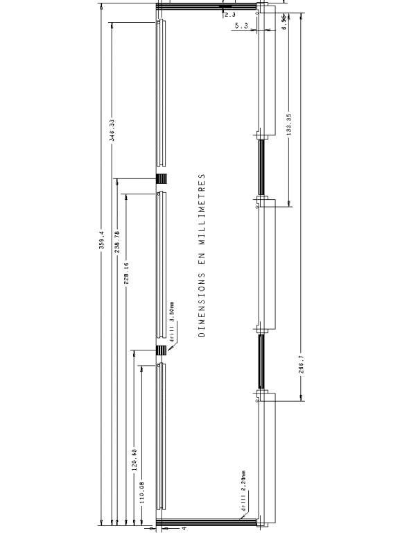
3.1. GIRV5 Card Dimensions.
3.2. PCB_AP board connections:
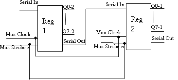
3.3. GIRV5 Shift registers connection figure
3.4. GIRV5 Dac and potentiometer connection figure