Notes for using the F2VB module.
This document describes the use of the F2VB front panel interconnections and handshakes to control the storage of data into the memory.
For VME software interface information refer to the ‘The Software Interface for the DT32-VME Buffer’ document obtainable from the Nuclear Physics Support Group document store at Web address :
http://nnsa.dl.ac.uk/MIDAS/documents/edoc239/edoc239.ps
A 34 pin IDC connector on the front panel inputs data as a 16 bit differential ECL bus into the memory. The data is stored in the memory in a 32 bit word format. The order of the 16 bit data in the 32 bit word is selected using a switch. The switch is position one of a six way DIL switch mounted on the F2VB PCB.
Switch ON: Selects the first data word to be in bit positions 16 -> 31, and the second data word bit positions 0 -> 15. The 32 bit word bit positions are defined as the VME data bus positions. I.e. bit 31 is MSB.
Switch OFF: Selects the first data word to be in bit positions 0 -> 15, and the second data word bit positions 16 -> 31. The 32 bit word bit positions are defined as the VME data bus positions. I.e. bit 31 is MSB.
If an odd number of 16 bit data is stored for an event, the F2VB inserts 16 bit data word in the remaining position in the 32 bit word. See section 6.0 for information on how select the inserted word.
These are the control signals available at the front panel as –ve Fast NIM, and differential ECL.
|
Signal Name |
Function. |
|
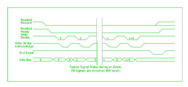
Readout Request |
Requests the F2VB for a Readout Ready signal to indicate the F2VB can accept data. Input to the F2VB. |
|
Readout Ready |
Indicates the F2VB can accept data. Output from the F2VB. |
|
Write Strobe |
The leading edge indicates data is valid on the Data bus. This signal should be removed in response to the leading edge of Write Strobe Acknowledge. Input to the F2VB. |
|
Write Strobe Acknowledge |
The leading edge indicates the F2VB has accepted the data from the Data bus. The signal will be removed when Write Strobe goes false. Output from the F2VB. |
|
End Event |
Indicates the end of the current Event, or data block. The signal should be true for a minimum of 50nS. The F2VB requires this signal to terminate storage, and allow internal buffer changes to take place. See ‘The Software Interface for the DT32-VME Buffer’ for further explanation. |
The front panel contains one 34 pin IDC connector, six LEMO00 sockets, and a 12 pin double row connector. The connections are described in the following tables.
Table 1: ECL control connections.
|
Connection name |
Interface Type |
Signal Description |
|
Spare |
Diffn. ECL |
Not used in this design. |
|
WSI |
Diffn. ECL |
Write Strobe Input terminated in 100 ohms. |
|
WACK |
Diffn. ECL |
Write Strobe Acknowledge output. Terminate in 100 ohms. |
|
RReq |
Diffn. ECL |
Readout Request input terminated in 100 ohms. |
|
Rready |
Diffn. ECL |
Readout Ready output. Terminate in 100 ohms. |
|
End-Event |
Diffn. ECL |
End-Event input terminated in 100 ohms. |
Table 2: NIM control connections.
|
Connection name |
Interface Type |
Signal Description |
|
Spare |
-ve Fast NIM |
Not used in this design. |
|
WSI |
-ve Fast NIM |
Write Strobe Input terminated in 50 ohms. |
|
WACK |
-ve Fast NIM |
Write Strobe Acknowledge output. Terminate in 50 ohms. |
|
RReq |
-ve Fast NIM |
Readout Request input terminated in 50 ohms. |
|
Rready |
-ve Fast NIM |
Readout Ready output. Terminate in 50 ohms. |
|
End-Event |
-ve Fast NIM |
End-Event input terminated in 50 ohms. |
There is one block of 12 jumpers, and one block of six switches. The function of these is described in the following table.
Jumpers 0 to 11 are used to select the A24 address base. A jumper missing requires the corresponding address be at logic 1 for access.
|
Jumper Number |
VME address bit |
Jumper Number |
VME address bit |
|
0 |
A12 |
6 |
A18 |
|
1 |
A13 |
7 |
A19 |
|
2 |
A14 |
8 |
A20 |
|
3 |
A15 |
9 |
A21 |
|
4 |
A16 |
10 |
A22 |
|
5 |
A17 |
11 |
A23 |
The function of the switch pack positions is described in this table.
|
Switch |
Function ‘ON’ |
Function ‘OFF’ |
|
1 |
Selects the first data word to be in bit positions 16 -> 31, and the second data word bit positions 0 -> 15. The 32 bit word bit positions are defined as the VME data bus positions. I.e. bit 31 is MSB. |
Selects the first data word to be in bit positions 0 -> 15, and the second data word bit positions 16 -> 31. The 32 bit word bit positions are defined as the VME data bus positions. I.e. bit 31 is MSB |
|
2 |
Sets Word insert select bit 0 to logic 0 |
Sets Word insert select bit 0 to logic 1 |
|
3 |
Sets Word insert select bit 1 to logic 0 |
Sets Word insert select bit 1 to logic 1 |
|
4 |
The front panel inputs control Readout Request. |
A permanent Readout Request is set. |
The words selected for inserting into a partially filled 32 bit word are selected according to the following table.
|
Word insert select code |
Word to be inserted |
|
00 |
0x1000000000000000 |
|
01 |
0x0000000000000000 |
|
10 |
0x1010101001010101 |
P.J.Coleman-Smith is the contact at Daresbury Laboratory in England for this module.
Email:
p.j.coleman-smith@dl.ac.ukMail: P.J.Coleman-Smith,
CLRC,
Daresbury Laboratory,
Daresbury,
Warrington.
WA4 4AD. England.
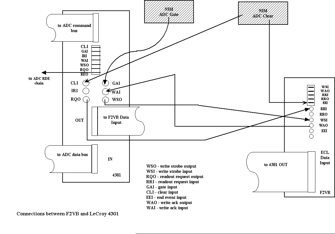
The diagram below shows a suggested connection scheme when the module is used with a LeCroy 4301 and LeCroy 4300 ADCs.