VME interface is A16/D16
Address space required is 256 bytes
Address selected using the jumpers STR1. Top is bit A8. A jumper installed is seen as a logic 0.
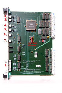
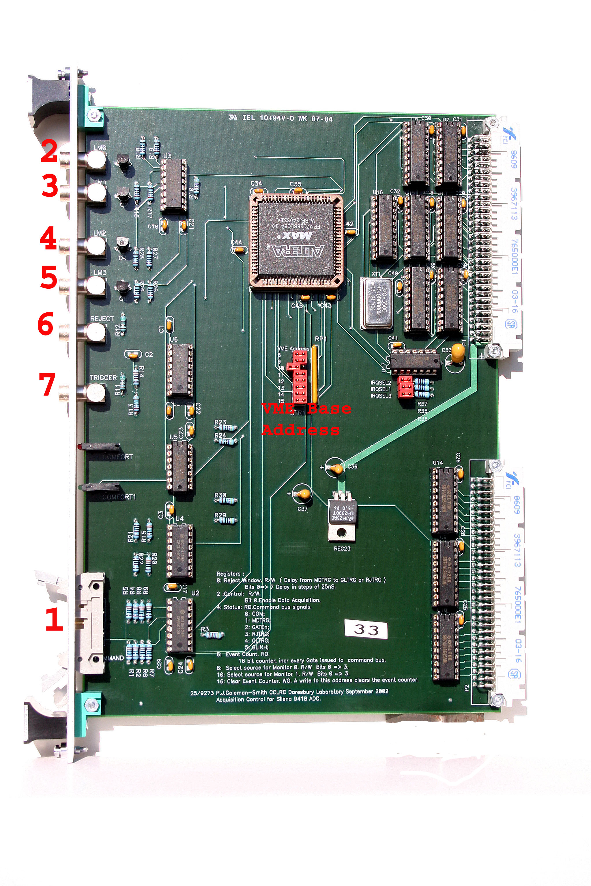
Silena 9418 Acquisition Control module
Function:
To control the Silena 9418 ADC modules attached to a front panel command bus.
A Trigger front panel input is connected to the Command bus COM line.
There is an 8 bit event counter which will be incremented only when an event is issued to the command bus.
Operation:
The Control register bit 0 ( Enable Data Acquisition ) controls the RJTRG line on the Command bus. When it is cleared any event in progress will complete, and no further events can take place. When it is set event collection by the ADCs can proceed.
The sequence for an event is as follows
1. Trigger input to Control module => COM signal on the command bus.
2. ADC accepts trigger => MDTRG signal on the command bus is set true. Also GLINH is set true.
3. Control module starts the Reject window delay counter.
4. Reject window counter completes. If the Reject signal is true then the RJTRG signal is set on the command bus.
If Reject is false then set the GLTRG on the command bus.
5. Wait for GLINH to be false ( all ADCs have completed conversion, or rejection of the event ).
6. If it was not a Reject, then increment the event counter.
7. Ready for the next event.
Hardware:
6U VME Format
VME interface is A16/D16
Address space required is 256 bytes
Address selected using the jumpers STR1. Top is bit A8. A jumper installed is seen as a logic 0.
You can obtain a full size high resolution version of the photograph here.
Front Panel connections:
Command bus interface (1). Differential ECL and Single ECL.
|
7. Trigger |
Fast NIM input |
|
6. Reject |
Fast NIM input |
|
2. Monitor 0 |
Fast NIM output |
|
3. Monitor 1 |
Fast NIM output |
|
4. Monitor 2 |
Fast NIM output |
|
5. Busy |
Fast NIM output ( Positive Logic ) - true when the ADCs are busy |
LEDS:
|
DTACK |
Red |
|
GLINH |
Red |
|
GLTRG |
Green |
|
ACQENB |
Green - Acquisition enable bit from Control register |
Hardware register address map:
The SAC is controlled by an ALTERA device and all information which follows is correct only for Altera firmware file acq_control_02july03_ss.tdf.
|
Offset |
Register |
Access |
Use |
|
0 |
DELR |
R/W |
Reject Window - Bits 0=>7. Delay in steps of 25ns |
|
2 |
CTRL |
R/W |
Bit 0: Enable Data Acquisition |
|
4 |
CBUS |
RO |
Command Bus signals |
|
6 |
EVCNT |
RO |
8 bit event counter |
|
8 |
MON2 |
R/W |
Bits 0=>3 Select source for Monitor 2 output |
|
16 |
EVCLR |
WO |
Clear Event Counter |
|
20 |
ARM |
WO |
A write to this address enables 1 event in Single Short Mode |
|
22 |
MON0 |
R/W |
Write 0 or 1 to set level of Monitor0 output |
Method of Use:
The Enable Data Acquisition bit (bit 0) of the CTRL register provides the overall Master Gate function needed when using more than one ADC module.
The Event Counter (EVCNT) is incremented only after the ADCs have finished processing an accepted COM signal (not BUSY). At this time the data for the event is now ready for readout from all ADC modules.
Software can poll the EVCNT register in order to detect an increment in its value which indicates that an event has occurred and is available for readout.
Software can use the output MON0 to produce a pulse (write 1 then 0 to the register) which can be used (for example) to RESET adcs if this is needed. [The S9418 does not require a RESET]
If a trigger signal is needed for other external data sources it should be taken from the COM signal issued by the SAC [Write 2 to register MON2] and not the trigger input to the SAC. In this way any other external data source only receives a trigger when an event is accepted by the S9418 ADCs. Also the Master Gate function of the SAC is then available to external data sources.
Data Acquisition can occur in two modes: buffered [write 1 to CTRL] and single shot [write 9 to CTRL].
In the buffered mode events occur while there is space in the S9418 FIFO data buffers. If one or more ADCs does not have space the BUSY signal is used to inhibit further triggers until software reads out the data. This mode of operation will give the lowest dead-time but can only be used if the data acquisition system consists only of a chain of S9418 modules.
In the single shot mode it is necessary for software to write to ARM before the SAC will accept a trigger and issue a COM signal. Software can then poll EVCNT until it is seen to increment. Event data from the S9418s can then be read togther with any other data from external data sources such as other VME ADCs, TDCs and scalers. Finally sofware must again write to ARM to enable the next event. In many cases it may be possible to use some overlap by ARMing the SAC immediately after an event is detected and before S9418 read-out. The software added dead-time can then be as low as 1-2 usec.
In single shot mode output Monitor 1 contains the Armed status.
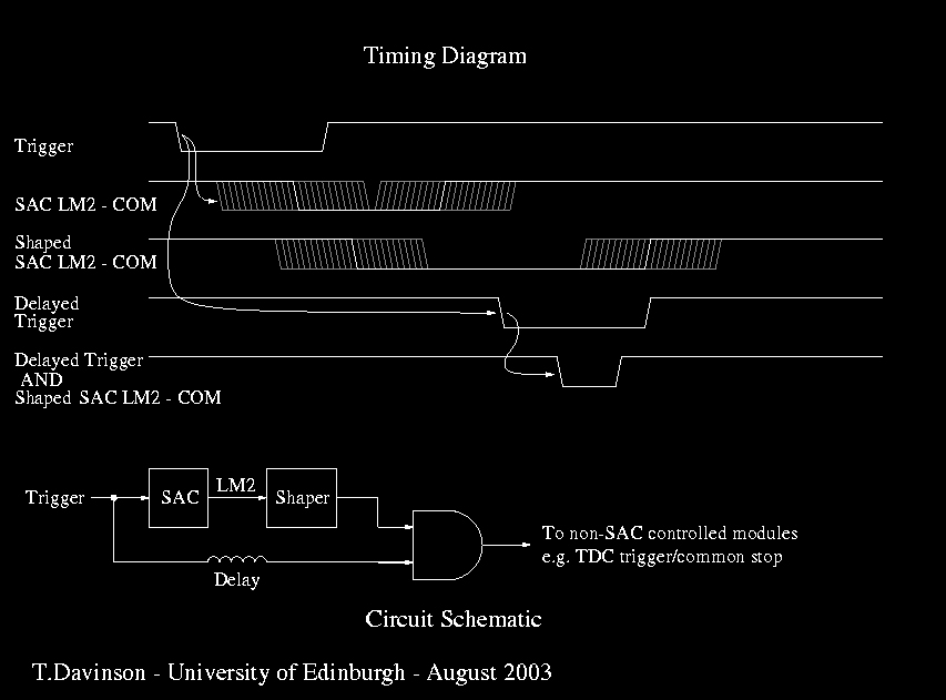
As a consequence of the 40MHz clock in the logic device used by the SAC there will be a 25ns jitter in the output COM signal generated
by the SAC as a result of an input trigger. In order to have a stable signal derived from the SAC COM which is needed as a source
of a trigger or gate for non-SAC controlled modules the following logic is suggested.
return to MIDAS download home page
![]()